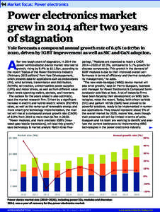
61 | Add to Reading ListSource URL: www.semiconductor-today.comLanguage: English - Date: 2015-04-08 17:14:33
|
|---|
62 | Add to Reading ListSource URL: www.semiconductor-today.comLanguage: English - Date: 2015-04-08 17:14:26
|
|---|
63 | Add to Reading ListSource URL: www.semiconductor-today.comLanguage: English - Date: 2015-01-23 09:11:01
|
|---|
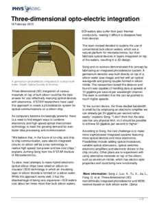
64 | Add to Reading ListSource URL: phys.orgLanguage: English - Date: 2015-04-17 00:22:08
|
|---|
65 | Add to Reading ListSource URL: manalis-lab.mit.eduLanguage: English - Date: 2011-02-10 14:18:35
|
|---|
66 | Add to Reading ListSource URL: manalis-lab.mit.eduLanguage: English - Date: 2011-02-10 14:18:35
|
|---|
67 | Add to Reading ListSource URL: www.lagunaclay.comLanguage: English - Date: 2010-12-13 10:23:55
|
|---|
68![IEEE ELECTRON DEVICE LETTERS, VOL. 34, NO. 4, APRIL[removed]Bottom-Gate Thin-Film Transistors Based on GaN Active Channel Layer IEEE ELECTRON DEVICE LETTERS, VOL. 34, NO. 4, APRIL[removed]Bottom-Gate Thin-Film Transistors Based on GaN Active Channel Layer](https://www.pdfsearch.io/img/3acfb91d2780965dd91db69a744f1725.jpg) | Add to Reading ListSource URL: www.pskl.ust.hkLanguage: English - Date: 2014-10-09 23:23:02
|
|---|
69![Growth and characterization of horizontal GaN wires on silicon Xinbo Zou, Xing Lu, Ryan Lucas, Thomas F. Kuech, Jonathan W. Choi, Padma Gopalan, and Kei May Lau Citation: Applied Physics Letters 104, [removed]); doi: Growth and characterization of horizontal GaN wires on silicon Xinbo Zou, Xing Lu, Ryan Lucas, Thomas F. Kuech, Jonathan W. Choi, Padma Gopalan, and Kei May Lau Citation: Applied Physics Letters 104, [removed]); doi:](https://www.pdfsearch.io/img/d34d38ce2940b5e721c3aca20f811ca9.jpg) | Add to Reading ListSource URL: ias.ust.hkLanguage: English - Date: 2014-08-19 04:51:40
|
|---|
70 | Add to Reading ListSource URL: www.nict.go.jpLanguage: English - Date: 2013-11-20 20:58:24
|
|---|